字数
3065 字
阅读时间
19 分钟
问题
Q1:不同bank里的MGTXTXP2_109 AJ4和IO_25_VRP_34有什么区别

A1:

Q2:不知道方向的 全部设置成input可以吗
input不需要定义 output需要接线,或者幅值 
Q3:ps端的jtag为什么接在了pl上

Q3:srio ip核创建方法
【高速接口-RapidIO】Xilinx SRIO IP 核详解-CSDN博客
Q4:分配引脚时有如下报错,可忽视

Q5:IO口管脚分配问题,分配管脚时遇到invalid placement site问题
是打开分配引脚的界面错误导致 


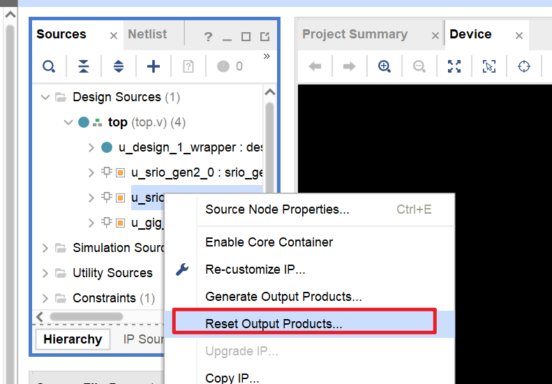
Q6:生成bit流失败,证书过期,加密ip核无法使用

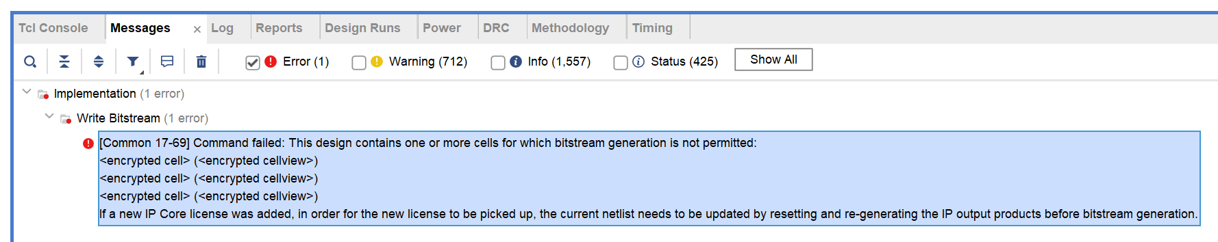 更新liscene以后还是没法使用,需要去官网申请,也无效 申请流程如下 [Common 17-69] Command failed: This design contains one or more cells for which bitstream generation-CSDN博客

 最后发现是补上加密的ip核的licence以后,


c
`timescale 1ns / 1ps
//////////////////////////////////////////////////////////////////////////////////
// Company:
// Engineer:
//
// Create Date: 2026/01/04 20:28:11
// Design Name:
// Module Name: Top
// Project Name:
// Target Devices:
// Tool Versions:
// Description:
//
// Dependencies:
//
// Revision:
// Revision 0.01 - File Created
// Additional Comments:
//
//////////////////////////////////////////////////////////////////////////////////
module top(
inout [14:0] DDR_addr ,
inout [2:0] DDR_ba ,
inout DDR_cas_n ,
inout DDR_ck_n ,
inout DDR_ck_p ,
inout DDR_cke ,
inout DDR_cs_n ,
inout [3:0] DDR_dm ,
inout [31:0] DDR_dq ,
inout [3:0] DDR_dqs_n ,
inout [3:0] DDR_dqs_p ,
inout DDR_odt ,
inout DDR_ras_n ,
inout DDR_reset_n ,
inout DDR_we_n ,
inout FIXED_IO_ddr_vrn ,
inout FIXED_IO_ddr_vrp ,
inout [53:0] FIXED_IO_mio ,
inout FIXED_IO_ps_clk ,
inout FIXED_IO_ps_porb ,
inout FIXED_IO_ps_srstb ,
output QSFP3_INTL ,
output QSFP3_RESETL ,
output QSFP3_SCL ,
output QSFP3_SDA ,
output MODSELL3 ,
output LPMOD3 ,
output MODPRSL3 ,
output LVDS_45_20_C_TXp1 ,
output LVDS_45_20_C_TXn1 ,
output LVDS_45_20_C_TXp2 ,
output LVDS_45_20_C_TXn2 ,
output LVDS_45_20_C_TXp3 ,
output LVDS_45_20_C_TXn3 ,
input LVDS_45_20_RXp1 ,
input LVDS_45_20_RXn1 ,
input LVDS_45_20_RXp2 ,
input LVDS_45_20_RXn2 ,
input LVDS_45_20_RXp3 ,
input LVDS_45_20_RXn3 ,
output LVDS_45_100_C_TXp1 ,
output LVDS_45_100_C_TXn1 ,
output LVDS_45_100_C_TXp2 ,
output LVDS_45_100_C_TXn2 ,
output LVDS_45_100_C_TXp3 ,
output LVDS_45_100_C_TXn3 ,
input LVDS_45_100_RXp1 ,
input LVDS_45_100_RXn1 ,
input LVDS_45_100_RXp2 ,
input LVDS_45_100_RXn2 ,
input LVDS_45_100_RXp3 ,
input LVDS_45_100_RXn3 ,
output UART_45_TX ,
input UART_45_RX ,
output A45_TRIG ,
output A1553B_45_D0 ,
output A1553B_45_D1 ,
output A1553B_45_D2 ,
output A1553B_45_D3 ,
output A1553B_45_D4 ,
output A1553B_45_D5 ,
output A1553B_45_D6 ,
output A1553B_45_D7 ,
output A1553B_45_D8 ,
output A1553B_45_D9 ,
output A1553B_45_D10 ,
output A1553B_45_D11 ,
output A1553B_45_D12 ,
output A1553B_45_D13 ,
output A1553B_45_D14 ,
output A1553B_45_D15 ,
input A1553B_45_A0 ,
input A1553B_45_A1 ,
input A1553B_45_A2 ,
input A1553B_45_A3 ,
input A1553B_45_A4 ,
input A1553B_45_A5 ,
input A1553B_45_A6 ,
input A1553B_45_A7 ,
input A1553B_45_A8 ,
input A1553B_45_A9 ,
input A1553B_45_A10 ,
input A1553B_45_A11 ,
output A1553B_45_A12 ,
input A1553B_45_A13 ,
input A1553B_45_A14 ,
input A1553B_45_N_INT ,
input A1553B_45_HRESET_N ,
input A1553B_45_NCS ,
input A1553B_45_NOE ,
input A1553B_45_NREADY ,
input A1553B_45_NWE ,
output RS485_45_TX_11 ,
output RS485_45_EN_11 ,
input RS485_45_RX_11 ,
output RS485_45_TX_12 ,
output RS485_45_EN_12 ,
input RS485_45_RX_12 ,
output RS485_45_TX_13 ,
output RS485_45_EN_13 ,
input RS485_45_RX_13 ,
output RS485_45_TX_21 ,
output RS485_45_EN_21 ,
input RS485_45_RX_21 ,
output RS485_45_TX_22 ,
output RS485_45_EN_22 ,
input RS485_45_RX_22 ,
output RS485_45_TX_23 ,
output RS485_45_EN_23 ,
input RS485_45_RX_23 ,
output RS485_45_TX_31 ,
output RS485_45_EN_31 ,
input RS485_45_RX_31 ,
output RS485_45_TX_32 ,
output RS485_45_EN_32 ,
input RS485_45_RX_32 ,
output RS485_45_TX_33 ,
output RS485_45_EN_33 ,
input RS485_45_RX_33 ,
output RS485_45_TX_41 ,
output RS485_45_EN_41 ,
input RS485_45_RX_41 ,
output RS485_45_TX_42 ,
output RS485_45_EN_42 ,
input RS485_45_RX_42 ,
output RS485_45_TX_43 ,
output RS485_45_EN_43 ,
input RS485_45_RX_43 ,
output RS485_45_TX_51 ,
output RS485_45_EN_51 ,
input RS485_45_RX_51 ,
output RS485_45_TX_52 ,
output RS485_45_EN_52 ,
input RS485_45_RX_52 ,
output RS485_45_TX_53 ,
output RS485_45_EN_53 ,
input RS485_45_RX_53 ,
output RS485_45_TX_61 ,
output RS485_45_EN_61 ,
input RS485_45_RX_61 ,
output RS485_45_TX_62 ,
output RS485_45_EN_62 ,
input RS485_45_RX_62 ,
output RS485_45_TX_63 ,
output RS485_45_EN_63 ,
input RS485_45_RX_63 ,
output RS485_45_TX_71 ,
output RS485_45_EN_71 ,
input RS485_45_RX_71 ,
output RS485_45_TX_72 ,
output RS485_45_EN_72 ,
input RS485_45_RX_72 ,
output RS485_45_TX_73 ,
output RS485_45_EN_73 ,
input RS485_45_RX_73 ,
output RS485_45_TX_81 ,
output RS485_45_EN_81 ,
input RS485_45_RX_81 ,
output RS485_45_TX_82 ,
output RS485_45_EN_82 ,
input RS485_45_RX_82 ,
output RS485_45_TX_83 ,
output RS485_45_EN_83 ,
input RS485_45_RX_83 ,
input RS422_45_RX_1 ,
output RS422_45_TX_1 ,
input RS422_45_RX_2 ,
output RS422_45_TX_2 ,
input RS422_45_RX_3 ,
output RS422_45_TX_3 ,
input RS422_45_RX_4 ,
output RS422_45_TX_4 ,
input RS422_45_RX_5 ,
output RS422_45_TX_5 ,
input RS422_45_RX_6 ,
output RS422_45_TX_6 ,
input RS422_45_RX_7 ,
output RS422_45_TX_7 ,
input RS422_45_RX_8 ,
output RS422_45_TX_8 ,
output PUDC_B ,
output SRIO1_TXp_0 ,
output SRIO1_TXn_0 ,
input SRIO1_RXp_0 ,
input SRIO1_RXn_0 ,
output SRIO1_TXp_1 ,
output SRIO1_TXn_1 ,
input SRIO1_RXp_1 ,
input SRIO1_RXn_1 ,
output SRIO1_TXp_2 ,
output SRIO1_TXn_2 ,
input SRIO1_RXp_2 ,
input SRIO1_RXn_2 ,
output SRIO1_TXp_3 ,
output SRIO1_TXn_3 ,
input SRIO1_RXp_3 ,
input SRIO1_RXn_3 ,
input Y3_156_25M_P ,
input Y3_156_25M_N ,
output SRIO3_TXp_0 ,
output SRIO3_TXn_0 ,
input SRIO3_RXp_0 ,
input SRIO3_RXn_0 ,
output SRIO3_TXp_1 ,
output SRIO3_TXn_1 ,
input SRIO3_RXp_1 ,
input SRIO3_RXn_1 ,
output SRIO3_TXp_2 ,
output SRIO3_TXn_2 ,
input SRIO3_RXp_2 ,
input SRIO3_RXn_2 ,
output SRIO3_TXp_3 ,
output SRIO3_TXn_3 ,
input SRIO3_RXp_3 ,
input SRIO3_RXn_3 ,
input Y2_156_25M_P ,
input Y2_156_25M_N ,
output SGMII_TXP_2 ,
output SGMII_TXN_2 ,
input SGMII_RXP_2 ,
input SGMII_RXN_2 ,
input Y5_125M_P ,
input Y5_125M_N
);
assign QSFP3_INTL = 'b0 ;
assign QSFP3_RESETL = 'b0 ;
assign QSFP3_SCL = 'b0 ;
assign QSFP3_SDA = 'b0 ;
assign MODSELL3 = 'b0 ;
assign LPMOD3 = 'b0 ;
assign MODPRSL3 = 'b0 ;
assign LVDS_45_20_C_TXp1 = LVDS_45_20_RXp1 ;
assign LVDS_45_20_C_TXn1 = LVDS_45_20_RXn1 ;
assign LVDS_45_20_C_TXp2 = LVDS_45_20_RXp2 ;
assign LVDS_45_20_C_TXn2 = LVDS_45_20_RXn2 ;
assign LVDS_45_20_C_TXp3 = LVDS_45_20_RXp3 ;
assign LVDS_45_20_C_TXn3 = LVDS_45_20_RXn3 ;
assign LVDS_45_100_C_TXp1 = LVDS_45_100_RXp1 ;
assign LVDS_45_100_C_TXn1 = LVDS_45_100_RXn1 ;
assign LVDS_45_100_C_TXp2 = LVDS_45_100_RXp2 ;
assign LVDS_45_100_C_TXn2 = LVDS_45_100_RXn2 ;
assign LVDS_45_100_C_TXp3 = LVDS_45_100_RXp3 ;
assign LVDS_45_100_C_TXn3 = LVDS_45_100_RXn3 ;
assign UART_45_TX = UART_45_RX ;
assign A45_TRIG = 'b0 ;
assign A1553B_45_D0 = A1553B_45_A0 ;
assign A1553B_45_D1 = A1553B_45_A1 ;
assign A1553B_45_D2 = A1553B_45_A2 ;
assign A1553B_45_D3 = A1553B_45_A3 ;
assign A1553B_45_D4 = A1553B_45_A4 ;
assign A1553B_45_D5 = A1553B_45_A5 ;
assign A1553B_45_D6 = A1553B_45_A6 ;
assign A1553B_45_D7 = A1553B_45_A7 ;
assign A1553B_45_D8 = A1553B_45_A8 ;
assign A1553B_45_D9 = A1553B_45_A9 ;
assign A1553B_45_D10 = A1553B_45_A10 ;
assign A1553B_45_D11 = A1553B_45_A11 ;
assign A1553B_45_D12 = 'b0 ;
assign A1553B_45_A12 = 'b0 ;
assign A1553B_45_D13 = A1553B_45_A13 ;
assign A1553B_45_D14 = A1553B_45_A14 ;
assign A1553B_45_D15 = A1553B_45_N_INT & A1553B_45_HRESET_N & A1553B_45_NCS & A1553B_45_NOE & A1553B_45_NREADY & A1553B_45_NWE ;
assign RS485_45_TX_11 = RS485_45_RX_11 ;
assign RS485_45_TX_12 = RS485_45_RX_12 ;
assign RS485_45_TX_13 = RS485_45_RX_13 ;
assign RS485_45_TX_21 = RS485_45_RX_21 ;
assign RS485_45_TX_22 = RS485_45_RX_22 ;
assign RS485_45_TX_23 = RS485_45_RX_23 ;
assign RS485_45_TX_31 = RS485_45_RX_31 ;
assign RS485_45_TX_32 = RS485_45_RX_32 ;
assign RS485_45_TX_33 = RS485_45_RX_33 ;
assign RS485_45_TX_41 = RS485_45_RX_41 ;
assign RS485_45_TX_42 = RS485_45_RX_42 ;
assign RS485_45_TX_43 = RS485_45_RX_43 ;
assign RS485_45_EN_11 = RS485_45_RX_11 ;
assign RS485_45_EN_12 = RS485_45_RX_12 ;
assign RS485_45_EN_13 = RS485_45_RX_13 ;
assign RS485_45_EN_21 = RS485_45_RX_21 ;
assign RS485_45_EN_22 = RS485_45_RX_22 ;
assign RS485_45_EN_23 = RS485_45_RX_23 ;
assign RS485_45_EN_31 = RS485_45_RX_31 ;
assign RS485_45_EN_32 = RS485_45_RX_32 ;
assign RS485_45_EN_33 = RS485_45_RX_33 ;
assign RS485_45_EN_41 = RS485_45_RX_41 ;
assign RS485_45_EN_42 = RS485_45_RX_42 ;
assign RS485_45_EN_43 = RS485_45_RX_43 ;
assign RS485_45_TX_51 = RS485_45_RX_51 ;
assign RS485_45_TX_52 = RS485_45_RX_52 ;
assign RS485_45_TX_53 = RS485_45_RX_53 ;
assign RS485_45_TX_61 = RS485_45_RX_61 ;
assign RS485_45_TX_62 = RS485_45_RX_62 ;
assign RS485_45_TX_63 = RS485_45_RX_63 ;
assign RS485_45_TX_71 = RS485_45_RX_71 ;
assign RS485_45_TX_72 = RS485_45_RX_72 ;
assign RS485_45_TX_73 = RS485_45_RX_73 ;
assign RS485_45_TX_81 = RS485_45_RX_81 ;
assign RS485_45_TX_82 = RS485_45_RX_82 ;
assign RS485_45_TX_83 = RS485_45_RX_83 ;
assign RS485_45_EN_51 = RS485_45_RX_51 ;
assign RS485_45_EN_52 = RS485_45_RX_52 ;
assign RS485_45_EN_53 = RS485_45_RX_53 ;
assign RS485_45_EN_61 = RS485_45_RX_61 ;
assign RS485_45_EN_62 = RS485_45_RX_62 ;
assign RS485_45_EN_63 = RS485_45_RX_63 ;
assign RS485_45_EN_71 = RS485_45_RX_71 ;
assign RS485_45_EN_72 = RS485_45_RX_72 ;
assign RS485_45_EN_73 = RS485_45_RX_73 ;
assign RS485_45_EN_81 = RS485_45_RX_81 ;
assign RS485_45_EN_82 = RS485_45_RX_82 ;
assign RS485_45_EN_83 = RS485_45_RX_83 ;
assign RS422_45_TX_1 = RS422_45_RX_1 ;
assign RS422_45_TX_2 = RS422_45_RX_2 ;
assign RS422_45_TX_3 = RS422_45_RX_3 ;
assign RS422_45_TX_4 = RS422_45_RX_4 ;
assign RS422_45_TX_5 = RS422_45_RX_5 ;
assign RS422_45_TX_6 = RS422_45_RX_6 ;
assign RS422_45_TX_7 = RS422_45_RX_7 ;
assign RS422_45_TX_8 = RS422_45_RX_8 ;
assign PUDC_B = 'b0 ;
design_1_wrapper u_design_1_wrapper(
.DDR_addr (DDR_addr ),
.DDR_ba (DDR_ba ),
.DDR_cas_n (DDR_cas_n ),
.DDR_ck_n (DDR_ck_n ),
.DDR_ck_p (DDR_ck_p ),
.DDR_cke (DDR_cke ),
.DDR_cs_n (DDR_cs_n ),
.DDR_dm (DDR_dm ),
.DDR_dq (DDR_dq ),
.DDR_dqs_n (DDR_dqs_n ),
.DDR_dqs_p (DDR_dqs_p ),
.DDR_odt (DDR_odt ),
.DDR_ras_n (DDR_ras_n ),
.DDR_reset_n (DDR_reset_n ),
.DDR_we_n (DDR_we_n ),
.FIXED_IO_ddr_vrn (FIXED_IO_ddr_vrn ),
.FIXED_IO_ddr_vrp (FIXED_IO_ddr_vrp ),
.FIXED_IO_mio (FIXED_IO_mio ),
.FIXED_IO_ps_clk (FIXED_IO_ps_clk ),
.FIXED_IO_ps_porb (FIXED_IO_ps_porb ),
.FIXED_IO_ps_srstb (FIXED_IO_ps_srstb )
);
srio_gen2_0 u_srio_gen2_0(
// Clocks and Resets
.sys_clkp (Y3_156_25M_P), // System reference clock
.sys_clkn (Y3_156_25M_N), // MMCM reference clock
.sys_rst (1'b1), // Global reset signal
// all clocks as output
.log_clk_out (), // LOG interface clock
.phy_clk_out (), // PHY interface clock
.gt_clk_out (),
.gt_pcs_clk_out (), // GT fabric interface clock
.drpclk_out (),
.refclk_out (),
.clk_lock_out (),
// all resets as output
.cfg_rst_out (),
.log_rst_out (), // Reset for LOG clock Domain
.buf_rst_out (),
.phy_rst_out (), // Reset for PHY clock Domain
.gt_pcs_rst_out (),
// QPLL outputs
.gt0_qpll_clk_out (),
.gt0_qpll_out_refclk_out (),
//---------------------------------------------
// Serial IO Interface
.srio_rxn0 (SRIO1_RXn_0), // Serial Receive Data
.srio_rxp0 (SRIO1_RXp_0), // Serial Receive Data
.srio_rxn1 (SRIO1_RXn_1), // Serial Receive Data
.srio_rxp1 (SRIO1_RXp_1), // Serial Receive Data
.srio_rxn2 (SRIO1_RXn_2), // Serial Receive Data
.srio_rxp2 (SRIO1_RXp_2), // Serial Receive Data
.srio_rxn3 (SRIO1_RXn_3), // Serial Receive Data
.srio_rxp3 (SRIO1_RXp_3), // Serial Receive Data
.srio_txn0 (SRIO1_TXn_0), // Serial Transmit Data
.srio_txp0 (SRIO1_TXp_0), // Serial Transmit Data
.srio_txn1 (SRIO1_TXn_1), // Serial Transmit Data
.srio_txp1 (SRIO1_TXp_1), // Serial Transmit Data
.srio_txn2 (SRIO1_TXn_2), // Serial Transmit Data
.srio_txp2 (SRIO1_TXp_2), // Serial Transmit Data
.srio_txn3 (SRIO1_TXn_3), // Serial Transmit Data
.srio_txp3 (SRIO1_TXp_3), // Serial Transmit Data
// LOG User I/O Interface
.s_axis_ireq_tvalid ('b0 ), // Indicates Valid Input on the Request Channel
.s_axis_ireq_tready ( ), // Beat has been accepted
.s_axis_ireq_tlast ('b0 ), // Indicates last beat
.s_axis_ireq_tdata ('b0 ), // Req Data Bus
.s_axis_ireq_tkeep ('b0 ), // Req Keep Bus
.s_axis_ireq_tuser ('b0 ), // Req User Bus
.m_axis_iresp_tvalid (), // Indicates Valid Output on the Response Channel
.m_axis_iresp_tready ('b0), // Beat has been accepted
.m_axis_iresp_tlast (), // Indicates last beat
.m_axis_iresp_tdata (), // Resp Data Bus
.m_axis_iresp_tkeep (), // Resp Keep Bus
.m_axis_iresp_tuser (), // Resp User Bus
.m_axis_treq_tvalid (), // Indicates Valid Output on the Response Channel
.m_axis_treq_tready ('b0), // Beat has been accepted
.m_axis_treq_tlast (), // Indicates last beat
.m_axis_treq_tdata (), // Resp Data Bus
.m_axis_treq_tkeep (), // Resp Keep Bus
.m_axis_treq_tuser (), // Resp User Bus
.s_axis_tresp_tvalid ('b0), // Indicates Valid Input on the Request Channel
.s_axis_tresp_tready (), // Beat has been accepted
.s_axis_tresp_tlast ('b0), // Indicates last beat
.s_axis_tresp_tdata ('b0), // Req Data Bus
.s_axis_tresp_tkeep ('b0), // Req Keep Bus
.s_axis_tresp_tuser ('b0), // Req User Bus
.s_axi_maintr_rst ('b0), // Reset for maintr interface, on LOG clk domain
// Maintenance Port Interface
.s_axi_maintr_awvalid ('b0), // Write Command Valid
.s_axi_maintr_awready (), // Write Port Ready
.s_axi_maintr_awaddr ('b0), // Write Address
.s_axi_maintr_wvalid ('b0), // Write Data Valid
.s_axi_maintr_wready (), // Write Port Ready
.s_axi_maintr_wdata ('b0), // Write Data
.s_axi_maintr_bvalid (), // Write Response Valid
.s_axi_maintr_bready ('b0), // Write Response Fabric Ready
.s_axi_maintr_bresp (), // Write Response
.s_axi_maintr_arvalid ('b0), // Read Command Valid
.s_axi_maintr_arready (), // Read Port Ready
.s_axi_maintr_araddr ('b0), // Read Address
.s_axi_maintr_rvalid (), // Read Response Valid
.s_axi_maintr_rready ('b0), // Read Response Fabric Ready
.s_axi_maintr_rdata (), // Read Data
.s_axi_maintr_rresp (), // Read Response
// PHY control signals
.sim_train_en ('b0), // Reduce timers for inialization for simulation
.force_reinit ('b0), // Force reinitialization
.phy_mce ('b0), // Send MCE control symbol
.phy_link_reset ('b0), // Send link reset control symbols
// core debug signals
.phy_rcvd_mce (), // MCE control symbol received
.phy_rcvd_link_reset (), // Received 4 consecutive reset symbols
.phy_debug (), // Useful debug signals
.gtrx_disperr_or (), // GT disparity error (reduce ORed)
.gtrx_notintable_or (), // GT not in table error (reduce ORed)
// side band signals
.port_error (), // In Port Error State
.port_timeout (), // Timeout value from Port Response Timeout CSR
.srio_host (), // Endpoint is the system host
// LOG Informational signals
.port_decode_error (), // Received transaction did not match a valid port
.deviceid (), // Device ID
.idle2_selected (), // The PHY is operating in IDLE2 mode
.phy_lcl_master_enable_out (),
.buf_lcl_response_only_out (),
.buf_lcl_tx_flow_control_out (),
.buf_lcl_phy_buf_stat_out (),
.phy_lcl_phy_next_fm_out (),
.phy_lcl_phy_last_ack_out (),
.phy_lcl_phy_rewind_out (),
.phy_lcl_phy_rcvd_buf_stat_out (),
.phy_lcl_maint_only_out (),
// PHY Informational signals
.port_initialized (), // Port is intialized
.link_initialized (), // Ready to transmit data
.idle_selected (), // The IDLE sequence has been selected
.mode_1x () // Link is trained down to 1x mode
);
srio_gen2_3 u_srio_gen2_3(
// Clocks and Resets
.sys_clkp (Y2_156_25M_P), // System reference clock
.sys_clkn (Y2_156_25M_N), // MMCM reference clock
.sys_rst (1'b1), // Global reset signal
// all clocks as output
.log_clk_out (), // LOG interface clock
.phy_clk_out (), // PHY interface clock
.gt_clk_out (),
.gt_pcs_clk_out (), // GT fabric interface clock
.drpclk_out (),
.refclk_out (),
.clk_lock_out (),
// all resets as output
.cfg_rst_out (),
.log_rst_out (), // Reset for LOG clock Domain
.buf_rst_out (),
.phy_rst_out (), // Reset for PHY clock Domain
.gt_pcs_rst_out (),
// QPLL outputs
.gt0_qpll_clk_out (),
.gt0_qpll_out_refclk_out (),
//---------------------------------------------
// Serial IO Interface
.srio_rxn0 (SRIO3_RXn_0), // Serial Receive Data
.srio_rxp0 (SRIO3_RXp_0), // Serial Receive Data
.srio_rxn1 (SRIO3_RXn_1), // Serial Receive Data
.srio_rxp1 (SRIO3_RXp_1), // Serial Receive Data
.srio_rxn2 (SRIO3_RXn_2), // Serial Receive Data
.srio_rxp2 (SRIO3_RXp_2), // Serial Receive Data
.srio_rxn3 (SRIO3_RXn_3), // Serial Receive Data
.srio_rxp3 (SRIO3_RXp_3), // Serial Receive Data
.srio_txn0 (SRIO3_TXn_0), // Serial Transmit Data
.srio_txp0 (SRIO3_TXp_0), // Serial Transmit Data
.srio_txn1 (SRIO3_TXn_1), // Serial Transmit Data
.srio_txp1 (SRIO3_TXp_1), // Serial Transmit Data
.srio_txn2 (SRIO3_TXn_2), // Serial Transmit Data
.srio_txp2 (SRIO3_TXp_2), // Serial Transmit Data
.srio_txn3 (SRIO3_TXn_3), // Serial Transmit Data
.srio_txp3 (SRIO3_TXp_3), // Serial Transmit Data
// LOG User I/O Interface
.s_axis_ireq_tvalid ('b0), // Indicates Valid Input on the Request Channel
.s_axis_ireq_tready (), // Beat has been accepted
.s_axis_ireq_tlast ('b0), // Indicates last beat
.s_axis_ireq_tdata ('b0), // Req Data Bus
.s_axis_ireq_tkeep ('b0), // Req Keep Bus
.s_axis_ireq_tuser ('b0), // Req User Bus
.m_axis_iresp_tvalid (), // Indicates Valid Output on the Response Channel
.m_axis_iresp_tready ('b0), // Beat has been accepted
.m_axis_iresp_tlast (), // Indicates last beat
.m_axis_iresp_tdata (), // Resp Data Bus
.m_axis_iresp_tkeep (), // Resp Keep Bus
.m_axis_iresp_tuser (), // Resp User Bus
.m_axis_treq_tvalid (), // Indicates Valid Output on the Response Channel
.m_axis_treq_tready ('b0), // Beat has been accepted
.m_axis_treq_tlast (), // Indicates last beat
.m_axis_treq_tdata (), // Resp Data Bus
.m_axis_treq_tkeep (), // Resp Keep Bus
.m_axis_treq_tuser (), // Resp User Bus
.s_axis_tresp_tvalid ('b0), // Indicates Valid Input on the Request Channel
.s_axis_tresp_tready (), // Beat has been accepted
.s_axis_tresp_tlast ('b0), // Indicates last beat
.s_axis_tresp_tdata ('b0), // Req Data Bus
.s_axis_tresp_tkeep ('b0), // Req Keep Bus
.s_axis_tresp_tuser ('b0), // Req User Bus
.s_axi_maintr_rst ('b0), // Reset for maintr interface, on LOG clk domain
// Maintenance Port Interface
.s_axi_maintr_awvalid ('b0), // Write Command Valid
.s_axi_maintr_awready (), // Write Port Ready
.s_axi_maintr_awaddr ('b0), // Write Address
.s_axi_maintr_wvalid ('b0), // Write Data Valid
.s_axi_maintr_wready (), // Write Port Ready
.s_axi_maintr_wdata ('b0), // Write Data
.s_axi_maintr_bvalid (), // Write Response Valid
.s_axi_maintr_bready ('b0), // Write Response Fabric Ready
.s_axi_maintr_bresp (), // Write Response
.s_axi_maintr_arvalid ('b0), // Read Command Valid
.s_axi_maintr_arready (), // Read Port Ready
.s_axi_maintr_araddr ('b0), // Read Address
.s_axi_maintr_rvalid (), // Read Response Valid
.s_axi_maintr_rready ('b0), // Read Response Fabric Ready
.s_axi_maintr_rdata (), // Read Data
.s_axi_maintr_rresp (), // Read Response
// PHY control signals
.sim_train_en ('b0), // Reduce timers for inialization for simulation
.force_reinit ('b0), // Force reinitialization
.phy_mce ('b0), // Send MCE control symbol
.phy_link_reset ('b0), // Send link reset control symbols
// core debug signals
.phy_rcvd_mce (), // MCE control symbol received
.phy_rcvd_link_reset (), // Received 4 consecutive reset symbols
.phy_debug (), // Useful debug signals
.gtrx_disperr_or (), // GT disparity error (reduce ORed)
.gtrx_notintable_or (), // GT not in table error (reduce ORed)
// side band signals
.port_error (), // In Port Error State
.port_timeout (), // Timeout value from Port Response Timeout CSR
.srio_host (), // Endpoint is the system host
// LOG Informational signals
.port_decode_error (), // Received transaction did not match a valid port
.deviceid (), // Device ID
.idle2_selected (), // The PHY is operating in IDLE2 mode
.phy_lcl_master_enable_out (),
.buf_lcl_response_only_out (),
.buf_lcl_tx_flow_control_out (),
.buf_lcl_phy_buf_stat_out (),
.phy_lcl_phy_next_fm_out (),
.phy_lcl_phy_last_ack_out (),
.phy_lcl_phy_rewind_out (),
.phy_lcl_phy_rcvd_buf_stat_out (),
.phy_lcl_maint_only_out (),
// PHY Informational signals
.port_initialized (), // Port is intialized
.link_initialized (), // Ready to transmit data
.idle_selected (), // The IDLE sequence has been selected
.mode_1x () // Link is trained down to 1x mode
);
gig_ethernet_pcs_pma_0 u_gig_ethernet_pcs_pma_0(
// Transceiver Interface
//----------------------
.gtrefclk_p (Y5_125M_P),
.gtrefclk_n (Y5_125M_N),
.gtrefclk_out (),
.gtrefclk_bufg_out (),
.txp (SGMII_TXP_2), // Differential +ve of serial transmission from PMA to PMD.
.txn (SGMII_TXN_2), // Differential -ve of serial transmission from PMA to PMD.
.rxp (SGMII_RXP_2), // Differential +ve for serial reception from PMD to PMA.
.rxn (SGMII_RXN_2), // Differential -ve for serial reception from PMD to PMA.
.resetdone (), // The GT transceiver has completed its reset cycle
.userclk_out (),
.userclk2_out (),
.rxuserclk_out (),
.rxuserclk2_out (),
.independent_clock_bufg ('b0),
.pma_reset_out (), // transceiver PMA reset signal
.mmcm_locked_out (), // MMCM Locked
// GMII Interface
//---------------
.sgmii_clk_r (),
.sgmii_clk_f (),
.sgmii_clk_en (), // Clock enable for client MAC
.gmii_txd ('b0), // Transmit data from client MAC.
.gmii_tx_en ('b0), // Transmit control signal from client MAC.
.gmii_tx_er ('b0), // Transmit control signal from client MAC.
.gmii_rxd (), // Received Data to client MAC.
.gmii_rx_dv (), // Received control signal to client MAC.
.gmii_rx_er (), // Received control signal to client MAC.
.gmii_isolate (), // Tristate control to electrically isolate GMII.
// Management: Alternative to MDIO Interface
//------------------------------------------
.configuration_vector ('b0), // Alternative to MDIO interface.
.an_interrupt (), // Interrupt to processor to signal that Auto-Negotiation has completed
.an_adv_config_vector ('b0), // Alternate interface to program REG4 (AN ADV)
.an_restart_config ('b0), // Alternate signal to modify AN restart bit in REG0
// Speed Control
//--------------
.speed_is_10_100 ('b0), // Core should operate at either 10Mbps or 100Mbps speeds
.speed_is_100 ('b0), // Core should operate at 100Mbps speed
// General IO's
//-------------
.status_vector ( ), // Core status.
.reset ('b0), // Asynchronous reset for entire core
.signal_detect ('b0), // Input from PMD to indicate presence of optical input.
.gt0_qplloutclk_out (),
.gt0_qplloutrefclk_out ()
);
endmodule贡献者
 dz13718198068